News All News
June 26th, 2023
Metalenz Launches its Metasurface Optics on the Open Market in Partnership with UMC
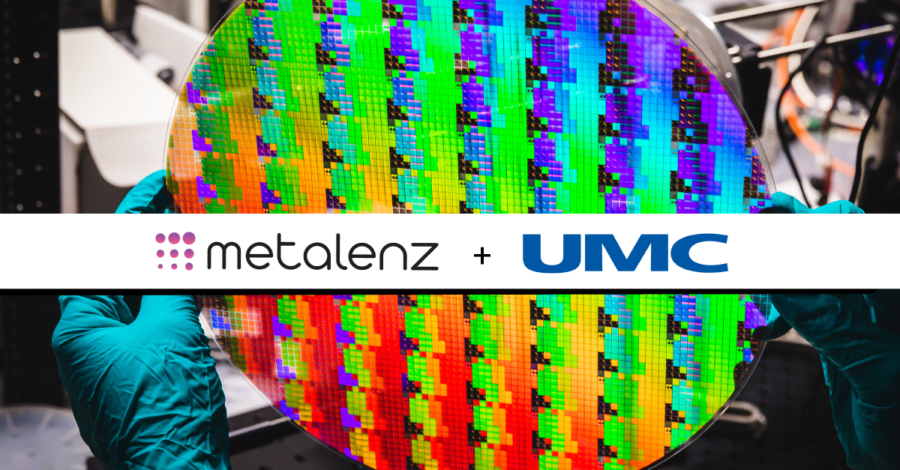
Metalenz has won several 3D depth sensing designs for its metasurface optics with leading OEMs in Asia. UMC has released Metalenz’s metasurface manufacturing process to production in its 12-inch wafer fab in Singapore. First commercial end-product shipments from OEMs begin Q3’23.

Boston, MA – June 26, 2023– Metalenz, the world leader in metasurface optics, today announced it has partnered with leading semiconductor foundry United Microelectronics Corporation (NYSE: UMC; TWSE: 2303) (“UMC”) to release its direct supply chain to mass production and bring the unrivaled scale and precision of semiconductor manufacturing to the optics industry. The announcement marks the launch of metasurface optics on the open market for the first time and follows multiple design wins for Metalenz with leading OEMs in Asia.
“After initially designing meta-optics in partnership with one of the leading suppliers of 3D sensing solutions, we are now engaged with OEMs directly to bring the benefits of metasurface optics to their 3D sensing applications. By partnering with a world-class foundry like UMC, we gain the manufacturing capabilities, expertise, and global reach to serve customers interested in adopting our meta-optics technology. This will further accelerate our growth as we are becoming the leading provider of precision optics for 3D sensing solutions.”
—Rob Devlin, Co-founder, and CEO of Metalenz.
“Our state-of-the art 12-inch facilities and decades of experience in semiconductor manufacturing has made us the foundry partner of choice for some of the most advanced fabless semiconductor companies in the world. Our expertise and scale will enable Metalenz to effortlessly scale up production to meet the growing demand for its meta-optics products,” said Raj Verma, Associate Vice President of Technology Development at UMC. “In the more-than-Moore era, UMC is focused on strengthening our specialty technology leadership to enable a wide range of 5G, IoT, and automotive applications. This collaboration will enable UMC to expand our offering into meta-optics and play a pioneering role in delivering this disruptive imaging technology to market.”
The partnership between Metalenz and UMC is expected to yield significant benefits for both companies and their customers. Metalenz’s meta-optic technology has the potential to revolutionize the field of optics, enabling the design of smaller, lighter, and more efficient optical systems. With the manufacturing capabilities provided by UMC, Metalenz will be able to accelerate the development of its meta-optic products and bring them to market more quickly as a direct supplier to OEMs.
The first designs to go through the newly established supply chain will be for Chinese OEM, DiluSense.
“As one of the most innovative suppliers of 3D sensing systems for IoT devices and consumer electronics we have been looking for better optics for years. We are excited to work with Metalenz, as their metasurface technology enables new optical form-factors and performance that will further differentiate some of our most advanced 3D sensing AI solutions.” Hu Lei, DiluSense Founder and CEO
About Metalenz
Metalenz, founded in 2016, is the first company to commercialize meta-optics. With exclusive worldwide license to the portfolio of foundational intellectual property relating to metasurfaces developed in the Capasso Lab at Harvard University, Metalenz has more than 20 patents on innovations that simplify and improve optical devices across multiple markets. The company’s metasurface technology provides complex, multifunctional optical performance in a single semiconductor layer, relocating large-scale production of optics to semiconductor foundries—printing lenses like computer chips. Following the successful June 2022 debut of its metasurface optics in time-of-flight systems for the consumer electronics market via a partnership with STMicroelectronics (NYSE: STM), and a $30 million series B funding round led by Neotribe Ventures announced in October 2022, the company continues to grow with millions of its metasurface optics now in market. Most recently, the Company’s PolarEyes™, a mobile form factor polarization imaging system, was recognized with a Prism Award in Cameras and Imaging from SPIE.
About UMC
UMC (NYSE: UMC, TWSE: 2303) is a leading global semiconductor foundry company. The company provides high quality IC fabrication services, focusing on logic and various specialty technologies to serve all major sectors of the electronics industry. UMC’s comprehensive IC processing technologies and manufacturing solutions include Logic/Mixed-Signal, embedded High-Voltage, embedded Non-Volatile-Memory, RFSOI and BCD etc. Most of UMC’s 12-in & 8-in fabs with its core R&D are in Taiwan, with additional ones throughout Asia. UMC has total 12 fabs in production with combined capacity of approximately 850,000 wafers per month (8-in equivalent), and all of them are certified with IATF 16949 automotive quality standard. UMC is headquartered in Hsinchu, Taiwan, plus local offices in United States, Europe, China, Japan, Korea & Singapore, with worldwide total 20,000 employees. For more information, please visit: umc.com
Press contact
Carly Glovinski
Marketing Manager, Metalenz
carly.glovinski@metalenz.com
Harvard’s Office of Technology Development entered into a license agreement with Metalenz for IP based on innovations developed in the Capasso Lab at Harvard University.
Tags: Harvard startups
Press Contact: Kirsten Mabry | (617) 495-4157
