Measuring resistance at the scale of a single transistor
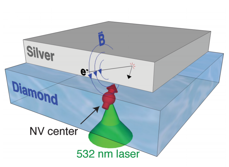
According to Moore’s law, electronic devices such as transistors have been shrinking in size to yield higher performance. Currently, feature sizes are on the order of 10 nm, and important parameters for the device operation, such as temperature and resistance, cannot be measured at this scale. This invention developed by Professor Lukin is a non-invasive probe using Nitrogen-Vacancy (NV) centers in diamond to measure temperature and resistance at resolutions of 10 nm - 100 nm enabling sensing, imaging, and control of classical and quantum mechanical devices at the nanoscale.

Schematic of example operation
U.S. Patent(s) Issued: 10,197,497
Case Number: 5726

