Unlocking High n+ Carrier Concentrations in Germanium for Advanced Devices
Germanium (Ge) holds great promise for the next generation of silicon CMOS-compatible devices due to its exceptional properties, including high electron and hole mobility and the ability to be grown directly on silicon substrates.
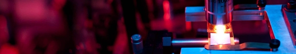
However, a persistent challenge in Ge device development has been achieving high n+ carrier concentrations through donor doping. Researchers at Harvard have developed a method to achieved a substantial n+ carrier concentration in strained epitaxial germanium-on-silicon. This work showcases that co-implantation and PLM can generate the necessary n+ carrier concentration and strain for high-performance Ge-on-Si devices, addressing the need for advanced methods in fabricating Ge films and related semiconductor structures.
This work was published in the Journal of Applied Physics.
U.S. Patent(s) Issued: US 10,541,136
Case Number: 6587