
Ice lithography for high resolution electron beam processing of fragile substrates
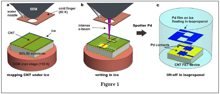
Electron beam lithography is a staple of microfabrication processes. The dominant practice, developed for silicon etching, first uses an organic photoresist to coat the substrate and then writes a desired pattern. However, this process can damage or contaminate substrates with fine features such as those employing carbon nanotubes and graphene. This invention uses ice layers to pattern a substrate for electon beam lithography and enables sub 20 nm resolution without damaging or contaminating the sample.
U.S. Patent(s) Issued: US 8,790,863
Case Number: 3940